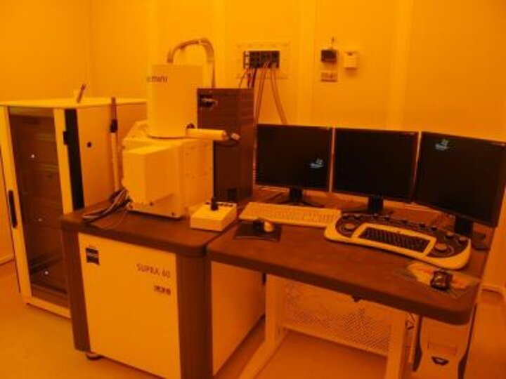
Electron Beam Lithography (EBL) System
This EBL system is composed with a Zeiss Supra 40 field-emission scanning electron microscope and a Raith pattern generator. The Zeiss Supra 40 features electron beam up to 30KeV and provides capability of reproducibly achieving feature sizes as small as 20nm. It is also integrated with an laser interferometer-controlled wafer stage, which makes it possible to accomplish stitching application and multilayer EBL with overlay accuracy better than 50nm on a wide variety of substrates.
Equipment Specification
- Energy of electrons: 0.1 - 30 keV
- Beam size (resolution): ~2.5 nm (~1.6 nm)
- Minimum pattern feature size: ~20 nm
- Field stitching accuracy: ~50 nm
- Maximum wafer size: 50mm×50mm
Positive Resists
- PMMA950-A4
- PMMA950-A9
- MMA(8.5) MMA EL6
- MMA(8.5) MMA EL11
- PMGI SF5
- PMGI SF11
Negative Resist
- FOx®-14 (HSQ)
Documents

Heidelberg DWL 66FS
Laser Lithography System
The Heidelberg DWL 66FS laser lithography system is a high resolution pattern generator for low volume mask making and direct writing on wafers. Using the autofocus function and the interferometer controlled high precision stage, it can write structures down to 0.6 μm with an address grid of 50 nm and multilayer exposure with accuracy up to 200 nm. The system can expose nearly all photo-resists by using a variety of different lasers. The capabilities and flexibility of this system make it the ultimate lithographic research tool in MEMS, BioMEMS, Micro Optics, Micro Fluidics, Sensors and all other applications.
Equipment Specifications
- 405nm, 60mW SSD laser source
- High resolution printing down to 0.6µm
- Overlay accuracy up to 0.2 µm
- Back to front side alignment
- Substrate size up to 200mm by 200mm
Positive Resists
- Shipley S-1813
- AZ-3312
- SPR220-7.0
- LOR-3A
- PMGI SF5
- PMGI SF11
Negative Resist
- MaN-1410

SUSS MicroTec MJB4
Mask Aligner
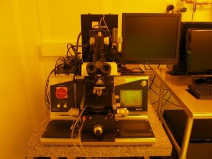
The MJB4 mask aligner is an easy to use instrument for high-resolution photolithography. It is equipped with UV exposure optics and lamps that allow a sub-micro exposure in vacuum contact. The achievable adjustment accuracy in X, Y direction is below 1 µm. The versatile mask holder allows both round and square plates as masks, and the sample plate accommodates small and odd-shaped substrates. Masks and wafer/substrates to a total thickness of 9.00 mm can be processed. The system also features an infrared system for backside or buried layer alignment.
Equipment Specification
- High resolution printing down to 0.8µm
- Overlay accuracy up to 1 µm
- Fast and accurate alignment with SUSS Single-field Microscope
- Backside infrared alignment
- Substrate size up to 100mm
Positive Resists
- Shipley S-1813
- AZ-3312
- SPR220-7.0
- LOR-3A
- PMGI SF5
- PMGI SF11
Negative Resist
- MaN-1410
Documents
